Close-up on Science
Simulations, microscopic images, artistic interpretations of research results, photos of instruments and more – our research often gives rise to fascinating pictures, a selection of which you can find on this page. They reflect the impressive variety of research topics and methods used at PGI.
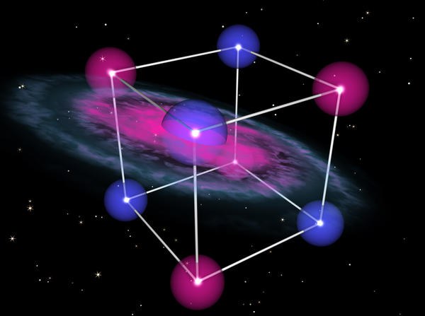
Building a European Quantum Computer in Jülich
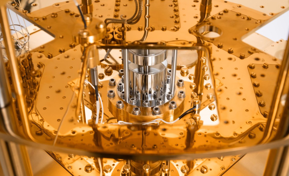
A European quantum computer with 50 to 100 superconducting qubits is to be developed and operated on our campus within the EU's Quantum Flagship Project OpenSuperQ. Scientists from across the world will have open access to it.
More information on the project "OpenSuperQ"
PGI research divisions:
Quantum computing
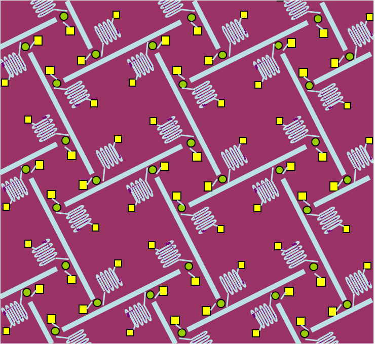
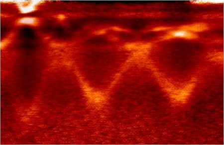
In modern computers, information is processed using bits. Quantum computers, however, work with qubits (quantum bits) and aim to carry out calculations which would be too demanding for today’s computers. Theoretical physicists at the Peter Grünberg Institute are looking for ways to establish the practical implementation of quantum information processing. The figure shows a detail from a two-dimensional integrated circuit component for error-tolerant quantum computing. The qubits are coloured green in the illustration.
IFF Spring School 2020 "Quantum Technology": www.iff-springschool.de
PGI research divisions:
Inside Insulator, Outside Conductor
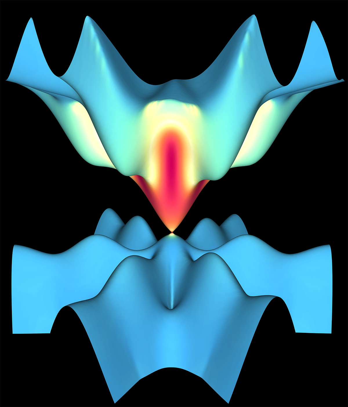
Topological insulators are novel materials with great potential for applications in information technologies. On the inside, they do not conduct electricity, but on their surfaces, electric currents can flow with less resistivity and heat emission than other conventional materials. Topological insulators are thus promising candidates for the development of faster and more energy-efficient computers and could prove to be the class of materials chosen as the basis for a new "green" information technology. Using advanced methods from theoretical physics in which the interactions between electrons in the material are treated quantum mechanically, PGI-1 simulates and analyzes the electronic properties of topological insulators. These studies aim to discover the most suitable materials for practical applications. The figure shows a 3-dimensional representation of the surface states of the topological insulator antimony telluride. The conical electron dispersion (shown in red), a so-called Dirac cone, is a typical feature of topological materials.
Original publication: Many-body corrected tight-binding Hamiltonians for an accurate quasiparticle description of topological insulators of the Bi2Se3 family; I. Aguilera et al.; Phys. Rev. B 100, 155147 - Published 30 October 2019
Research division: Quantum Theory of Materials(PGI-1/IAS-1)
Vacancies in Crystalline Phase-change Materials
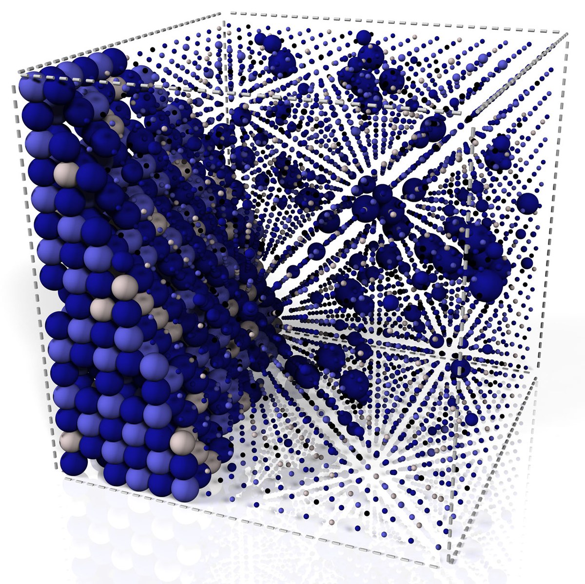
Density Functional Theory study of the role of vacancies on the electronic structure in crystalline phase-change materials employing the recently developed KKRnano method on the BlueGene/P supercomputer JUGENE using a cubic supercell of 4096 atoms containing Ge512VAC512Sb1024Te204.
The figure displays the atomically resolved spatial distribution of local density of states (LDOS) at the Fermi energy. In the left lower part the chemical information, in the upper right part the value of the LDOS is displayed. Here, large (small) radii of the spheres correspond to high (low) DOS values. For both parts of the plot Ge, Vac, Sb, and Te are shown in white, transparent, light blue, and dark blue, respectively.
Original publication:
Zhang, W. ; Thiess, A. ; Zalden, P. et al.;
Role of vacancies in metal-insulator transitions of crystalline phase-change materials;
Nature materials 11 (2012) 952 – 956
More information on KKRnano
Seeking the Fourth Property of Electrons
Researchers at the Peter Grünberg Institute are trying, in collaboration with colleagues from the USA and the Czech Republic, to establish proof of an electric dipole moment in electrons. Its existence is a precondition for the accuracy of several theories in physics, connected, for example, with the origin of the universe. In order to improve the accuracy of previous measurements, researchers have produced a new ceramic material with the help of the Jülich Supercomputer JUROPA.
Original publication:
A multiferroic material to search for the permanent electric dipole moment of the electron;
K. Z. Rushchanskii et al.;
Nature Materials (2010), DOI: 10.1038/NMAT2799
Press release: Researchers Seeking the Fourth Property of Electrons
Young investigator’s group: Computational Nanoferronics Laboratory
Tracking down Electrons
The figure here shows a section through the electron distribution within the chemical element tungsten. The colour intensity marks the density in the distribution of electrons; the lighter the area, the more electrons are present. An international research team including scientists from the Peter Grünberg Institute have successfully managed to investigate the electronic state of crystalline materials at a level more than ten times deeper inside the materials as was previously possible. Due to the fact that the physical properties of solids are based on just these electronic states in the inner part of materials, the method is predicted to have considerable potential for materials research.
Original publication:
Probing bulk electronic structure with hard X-ray angle-resolved photoemission;
A.X. Gray et al;
Nature Materials (2011), DOI:10.1038/nmat3089
Press release: Breakthrough in Photoemission Spectroscopy
Research division:"Electronic Properties" (PGI-6)
Magnetic Vortices
Magnetic spirals occur in nanometer-thin magnetic layers. The magnetization of the nucleus of these spirals can be switched at lightning speed when a short electric pulse is applied – a process shown here in this computer simulation. Structures such as these could function as bits in miniaturized data storage systems of the future.
Research division: "Electronic Properties" (PGI-6)
Nano-Sonar
Just as a sonar device sends out sound waves in order to explore the hidden depths of the ocean, electrons can be used in the same way by scanning tunnelling microscopes to investigate the concealed properties of the atomic lattice of metals.
Original publication:
Seeing the Fermi Surface in Real Space by Nanoscale Electron Focusing;
Weismann et al.; Science (2009), DOI: 10.1126/science.1168738
Presse release: Nano-Sonar Uses Electrons to Measure under the Surface
Young investigators group:"Functional Nanoscale Structure Probe and Simulation Laboratory":
Multi-purpose Tool for Spintronics Research
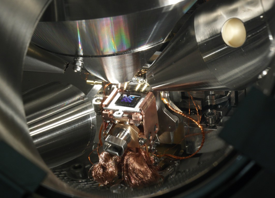
In search of energy-efficiency in information technology of the future, scientists at the Peter Grünberg Institute create and research into nanoscale components for spintronics. They are aided in their task by the “Swiss Army knife” of research tools: using this custom-designed “Nano-Spintronics-Cluster-Tool”, researchers can produce, display and investigate nanocomponents in ultra-high vacuum. The photograph shows a detail of this specialist tool, which weighs around three tons.
More information: Nano-Spintronics-Cluster-Tool
Analysing Electrochemistry on the Atomic Level
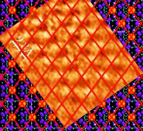
Researchers at the Peter Grünberg Institute, together with scientists from Aachen, Germany, and Tsukuba, Japan, have discovered a new way of studying electrochemical processes on the atomic scale. This method could help to improve the energy efficiency of systems, which should in the future enable a new form of fast and energy-saving storage in information technology. In addition, the methodology opens up new opportunities for the investigation and optimization of fuel cells, batteries, chemical sensors and catalysts. The image here shows the atomic resolution of the structure of a solid electrolyte.
Original publication:
Atomically controlled electrochemical nucleation at superionic solid electrolyte surfaces;
I. Valov et al.; Nature Materials (2012), DOI: 10.1038/NMAT3307
Press release from 29.04.2012 “Electrochemistry on the Atomic Level”
Electron Waves
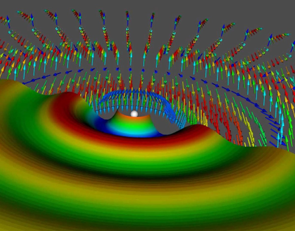
Physicists at the Peter Grünberg Institute have discovered a new magnetic state with the help of computer simulations. It occurs when a magnetic impurity atom is deposited on the surface of a metal. As the electrons of the metal interact with the magnetic field of the impurity atom, ring-shaped waves made up of electrons develop on the surface of the metal. They resemble the waves which form on the surface of a body of water when a stone is dropped into it.
Original publication:
Magnetic adatom induced skyrmion-like spin texture in surface electron waves;
Lounis et al.; Physical Review Letters (2012), DOI: 10.1103/PhysRevLett.108.207202
Young investigators group “Functional Nanoscale Structure Probe and Simulation Laboratory”
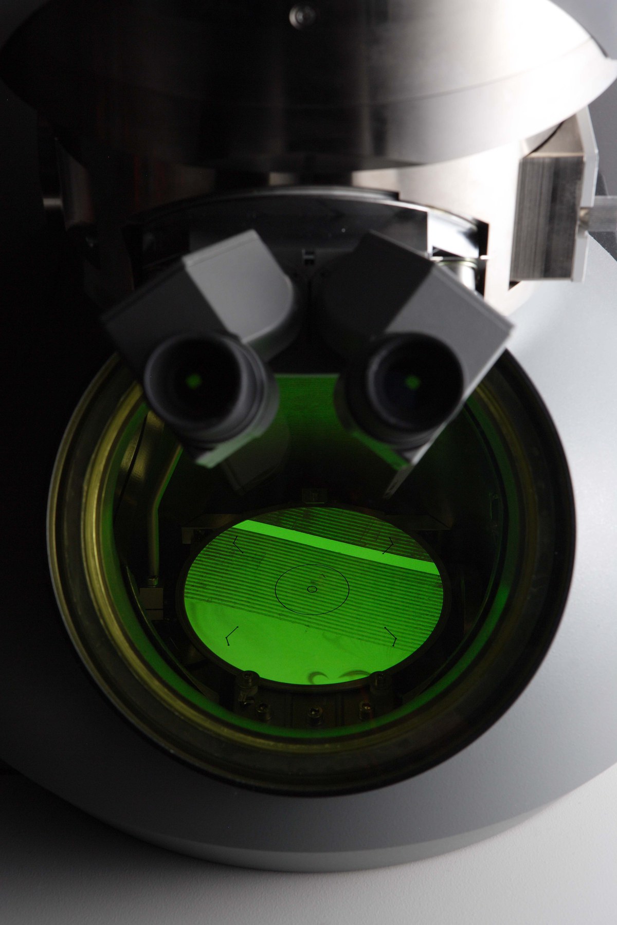
Research with Neutrons
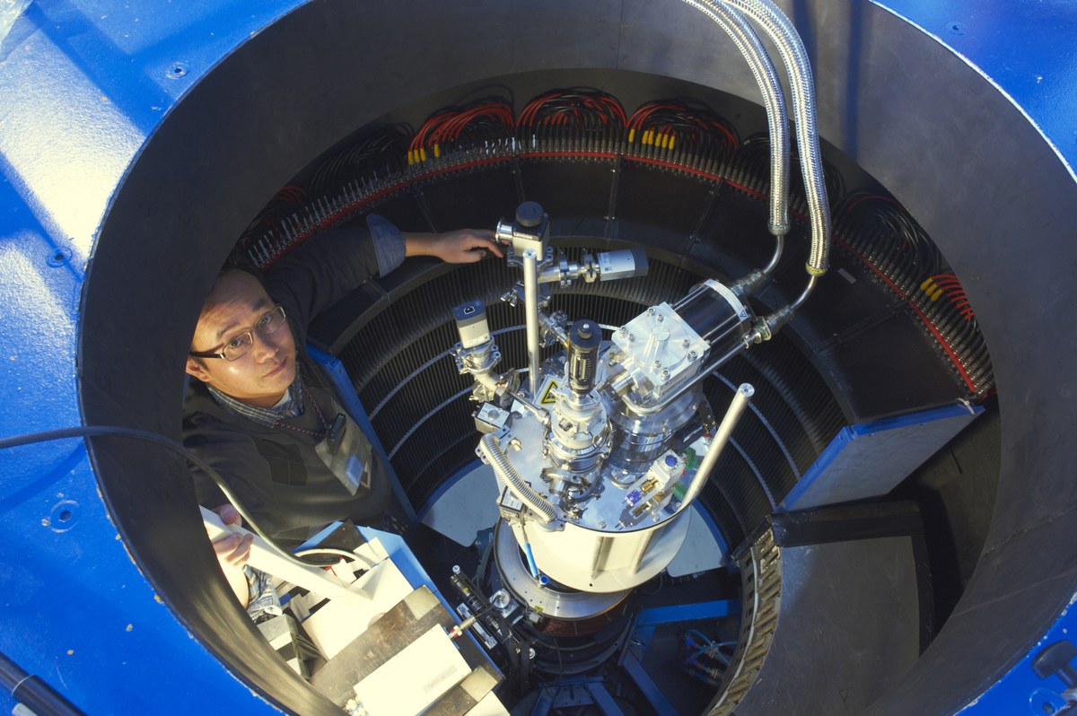
Researchers at the Jülich Centre for Neutron Science and the Peter Grünberg Institute can, with the help of neutrons, investigate the atomic construction and movements of materials with great precision. Using the “spectrometer for diffuse neutron scattering”, shown here in the picture, it is possible, for example, to detect the magnetic structure of nanomaterials with atomic precision. Such materials should some day find a use in highly efficient data storage systems in information technology or for quantum computers.
Read more: DNS - Spectrometer for diffuse scattering
A Microscope Films a Microscope in Operation

A scanning tunnelling electron microscope detects nanostructures atom by atom. A video from the Peter Grünberg Institute shows how the ultrafine tip of this type of microscope scans the surface of a sample. This was “filmed” using a scanning electron microscope.
Nanowires Made from Semiconductor Material
Using the so-called bottom-up approach, semiconductor nanostructures can be produced directly by means of epitaxial growth. In contrast to the alternative top-down method, where lithographical processes are laboriously defined, this approach has the potential to simplify the fabrication process considerably. Among the possible structures which can be fabricated using the bottom-up approach, semiconductor nanowires, such as the ones shown here, are of special interest. The associated one-dimensional electrical channel can be used, not only as a building block for future nanotransitors, but also as a versatile basis for diverse quantum structures.
Research division:Semiconductor Nanoelectronics (PGI-9)
Molecular Magnets
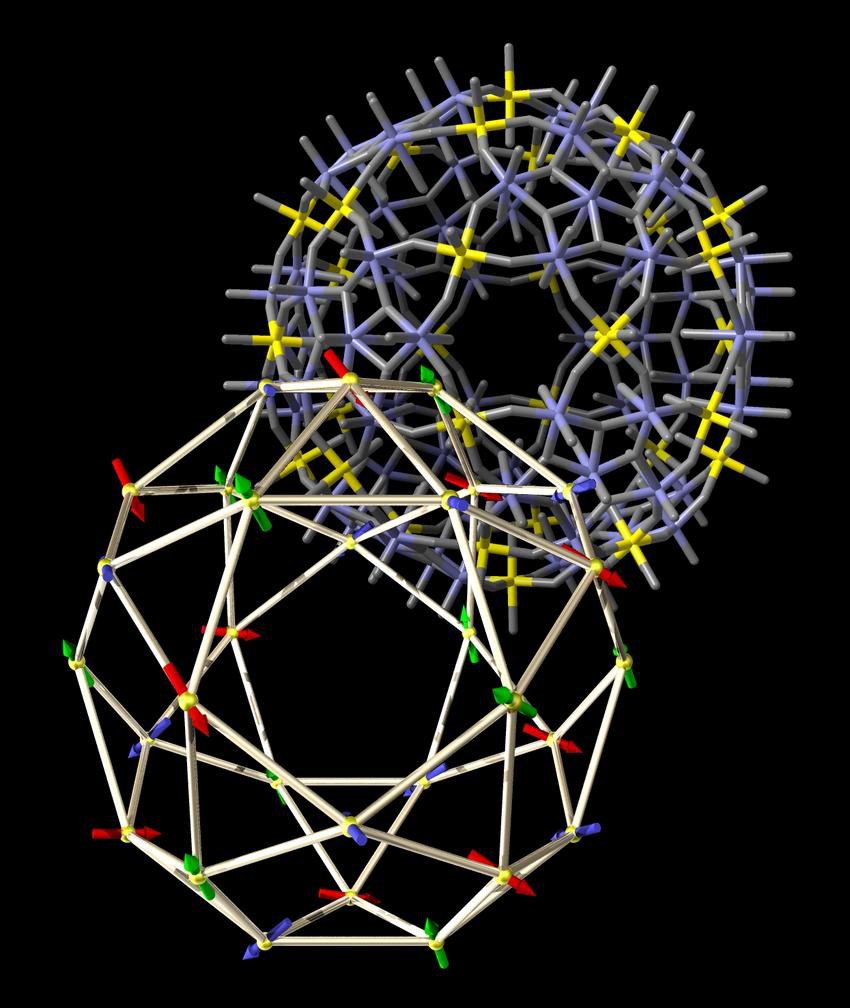
The image shows polyocometallat {Mo72Fe30}, a spherical molecule with 30 magnetic centres. This type of magnetic molecule with nanoscale dimensions should one day be useful for highly efficient data storage in the field of information technology or in quantum computing.
Research in nanomagnetism at the research divisions
(Quantum Materials and Collective Phenomena (PGI-4/JCNS-2)
and Electronic Properties (PGI-6)
Nanopositioners

Researchers at the Peter Grünberg Institute have developed a piezoelectric motor, with a diameter of less than 2.5 millimetres. Due to the motor’s compact size, scientists can install up to four of these so-called “Koala drives” in a single scanning tunnelling microscope, and thus access samples simultaneously using multiple tips. This makes it possible, for example, to undertake detailed investigations of charge transport in nanostructures.
More: Scanning probe microscopy with the “Koala drive”
Ultrahigh-resolution Electron Microscopy
Ultrahigh-resolution transmission electron microscopy nowadays enables inter-atomic distances in materials to be measured with an accuracy of a few picometres. A picometre is approximately one hundred times smaller than the diameter of an atom. In this way, it is possible to identify the decisive parameters that determine the physical properties of materials directly on the atomic level in a transmission electron microscope. Such studies are only possible at a few locations in the world. The Ernst Ruska-Centre for Microscopy and Spectroscopy with Electrons in Forschungszentrum Jülich is one of the pioneers in this area of research.
Research division:
Electron microscopy at the research division: ER-C-1
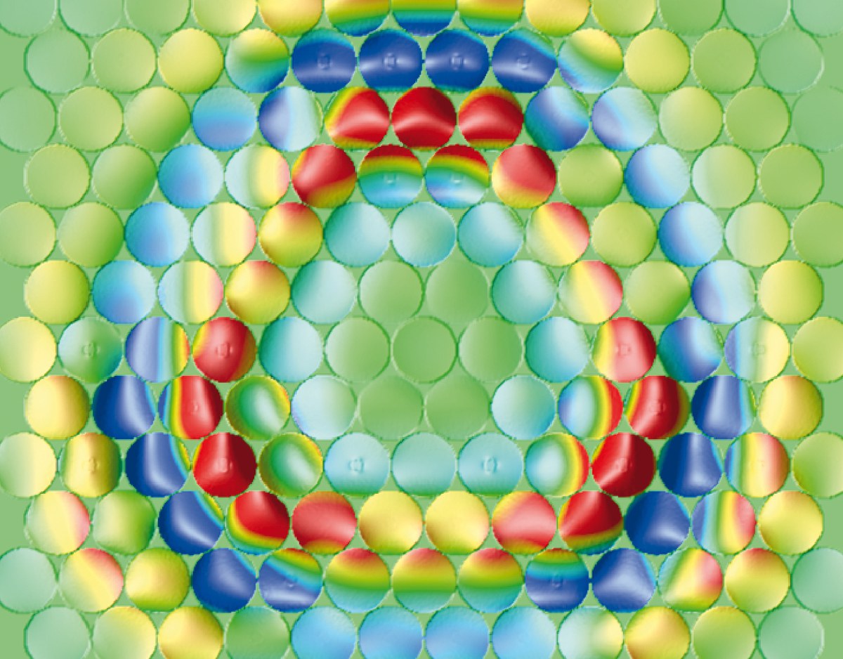
Collective Phenomena
Certain physical phenomena only exist as a result of the interplay of a multitude of particles. Waves, for example, cannot be generated from just a single water molecule. Researchers at the Peter Grünberg Institute are investigating this type of so-called “correlated” phenomena in solids, arising from the interaction of hundreds of billions of atomic nuclei and electrons. One of the challenges of their work is that the properties they are looking for do not derive directly from the basic formulae of elementary particle physics; here, the whole is clearly far more than the sum of its parts.
Research divisions:
Quanten-Theorie der Materialien (PGI-1 / IAS-1)
Theoretische Nanoelektronik (PGI-2 / IAS-3)
Streumethoden (PGI-4 / JCNS-2)
Image taken from: How chemistry controls electron localization in 3d1 perovskites: a Wannier-function study;
Pavarini et al.; New J. Phys. 7 188, DOI:10.1088/1367-2630/7/1/188
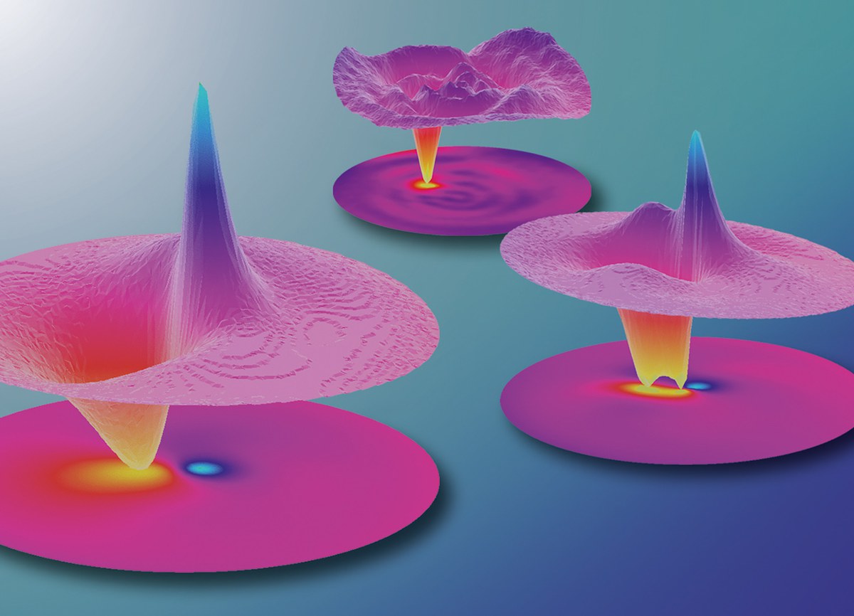
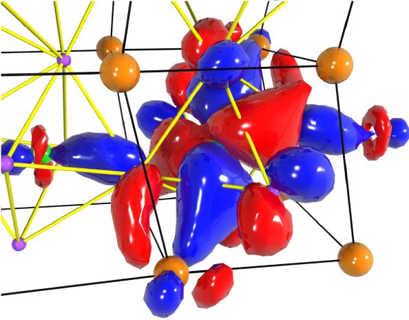
Single-molecule Electronic Devices
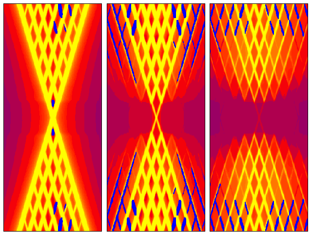
With miniaturization increasing in the field of information technology, the idea of using single molecules as tiny electronic components is becoming ever more appealing. Researchers at the Peter Grünberg Institute are studying the quantum transport properties of such molecules. Using methods from theoretical physics, such as quantum field theory and statistical mechanics, they investigate, for example, magnetic molecules such as metallic-organic complexes. When electric or magnetic fields are applied, these molecules react with charge, spin and vibrational excitations. A better understanding of the resulting effects and their interplay could make a variety of novel technical applications possible. The above image illustrates the effect of the vibration of a molecular device on its conductance.
Research division:Theoretical Nanoelectronics (PGI-2/IAS-3)
How the "PICO" Microscope Works
With the help of the best electron microscopes of our times, at the Ernst Ruska-Centre researchers are able to model and examine in great detail the arrangement of atoms in a material, including how the interplay of atoms determines the properties of materials as well as components and circuits. In February 2012, the ER-C added a high-performance microscope unique in Europe to its inventory of equipment; the PICO is able to correct not just spherical aberrations but also another type of lens defect – known as chromatic aberration – and in doing so is able to achieve a record resolution of 50 billionths of a millimetre.
See how the PICO works in this video
Read more about “PICO” (Advanced Picometre Resolution Project) in our brochure Insight into the World of Atoms (PDF, 9 MB)
Ernst Ruska-Centrum (ER-C): www.er-c.org
Surface States of Semiconductor Nanowires
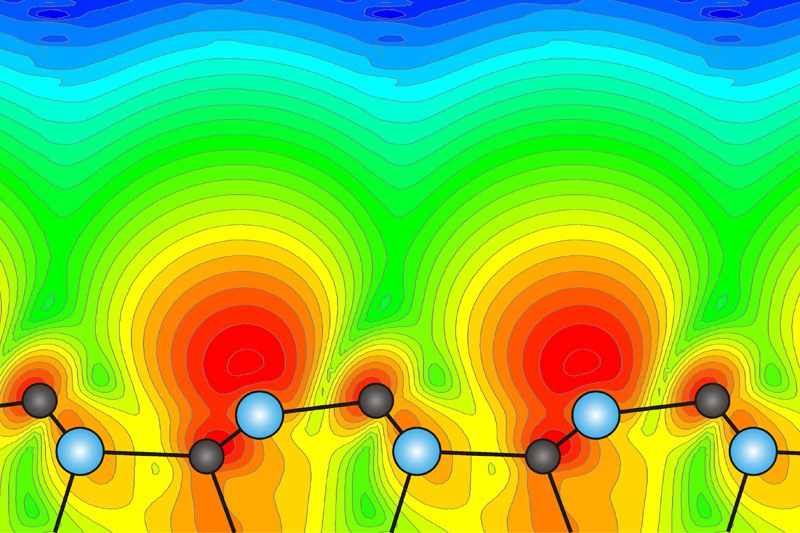
PGI-5 researchers have made a significant contribution to elucidating the surface structure of gallium nitride nanowires. Their findings are also likely to be applicable to nanowires made from other semiconductors, providing fresh impetus for the development of miniature optoelectronic components. The image illustrates the density of states at the surface of a gallium nitride crystal (below) under vacuum, and thus the probability that the electrons take on certain energy levels (red = high, green = low).
Original publication:
Hidden surface states at non-polar GaN (1010) facets: Intrinsic pinning of nanowires; L. Lymperakis et al.; Appl. Phys. Lett. 103, 152101 (2013), published online 7 October 2013, DOI: 10.1063/1.4823723, Article
Research division:: Microstructur Research(ER-C-1 / PGI-5)
Counting on Neodymium
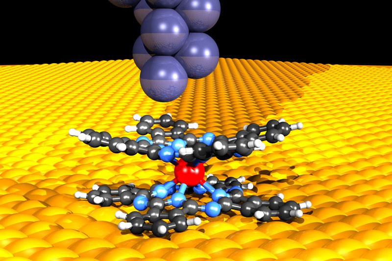
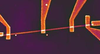
Magnetic molecules are regarded as promising functional units for the future of information processing. An interdisciplinary team of researchers from the Peter Grünberg Institute and RWTH Aachen University were the first to produce particularly robust magnetic molecules that enable a direct electrical readout of magnetic information. This was made possible by selecting the rare earth metal neodymium as the central building block of the molecule. The image shows the tip of a scanning tunnelling microscope (above), which the researchers use to conduct electric current through a magnetic double-decker molecule placed on a copper layer (below). A neodymium atom (red) is located at the centre of the molecule.
Original publication
Accessing 4f-states in single-molecule spintronics;
S. Fahrendorf et al.; Nature Communications, published online 24 September 2013, DOI: 10.1038/ncomms3425, Artikel
Press release: Counting on Neodymium - Promising candidate for information processing with magnetic molecules
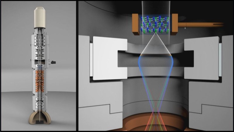
Feasibility of Quantum Computing
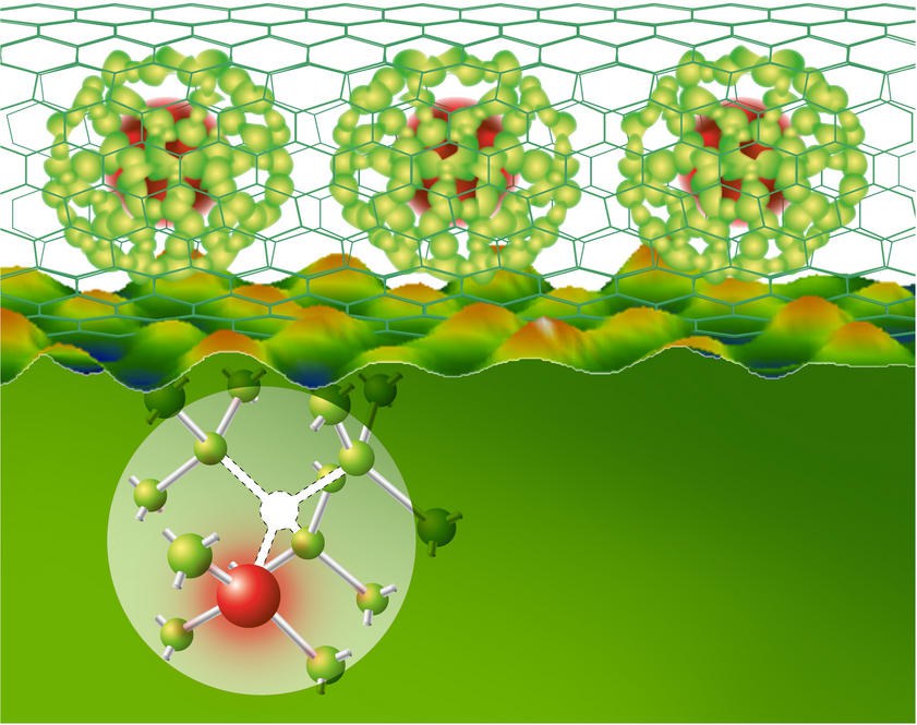
“Peapods” such as these should help in the implementation of quantum computing. A “pea pod” is made up of a tiny carbon nanotube filled with fullerenes, spheres made from carbon atoms. Each sphere contains a nitrogen atom, whose spin then serves as an arithmetic unit. The carbon atoms themselves have no spin and therefore stabilize the nitrogen spin. The “peapods” are placed on a diamond containing nitrogen defects. These can be read out optically and receive spin information from the qubits through coupling.
News from 14. November 2012: ”PGI Researchers Work on the Feasibility of Quantum Computing”
Projects undertaken by the research group “Spintronics in Carbon Nanostructures”