Jonas Mair - DR project
Energy efficient digital technologies for scalable Quantum Computing
Doctoral Researcher: Jonas Mair
Local ZEA-2 Supervisor: Lammert Duipmans
Topic: Quantum Computing
Research Field: Information
Motivation and Target
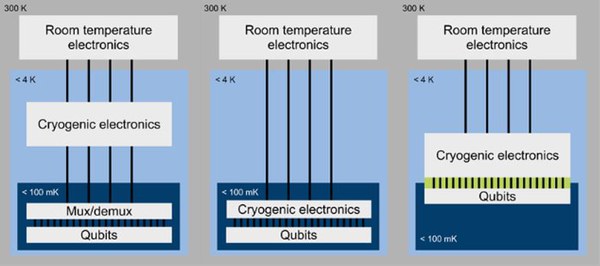
For a universal quantum computer becoming practical, it needs millions of qubits that are tuned, controlled and read out. Complex tuning and error correction algorithms have to be run to extract a valid computational result. On the road to these amounts of qubits, one has to think about scaling the overall system, including the connections to the qubits, the hardware that interfaces it and the software that controls it.
Our strategy at ZEA-2 to scale is to combine semiconducting qubits with integrated chips close by on the lower temperature stages. This allows for tight integration and control of the qubits while leveraging modern IC fabrication processes. However, the controlling ICs use up power and therefore heat up the environment of the qubits. Resulting from that is a reduced qubit fidelity. Therefore heat becomes a new scaling bottleneck.
The idea of this project is to find energy efficient digital technologies profiting from the cryogenic environment to reduce the heating up in the vicinity of the qubits. Additionally, digital design processes should be improved for cryogenic IC design.
Strategy
After years of digital design and fabrication process the industry stabilized to a logic gate implementation with a pull up network of PMOS FETs in combination with a pull down network of NMOS FETs, called complementary MOS (CMOS). Advantages of this design are speed and density, both desirable for modern high performance ICs. The cryogenic environment however levels the playing field, by on the one hand strict power requirements but on the other hand different environmental conditions.
The strategy is to reevaluate and compare logic families filtered in the development to the current one on their suitability for a cryogenic environment while also possibly coming up with new logic families specifically designed for it. The families should be ranked according to the timeframe it would take to adopt them, as tooling and design paradigms specialized on the current variant need to be adapted. As such there are 3 timespans defined, short-term (5-10 years), mid-term (10-15 years) and long-term (15-20 years).
As an example: Adiabatic logic [2] is an interesting contender, as it allows for a theoretical power draw tending towards zero for low frequencies. But it also requires a wildly different approach to digital IC design.
References
[1] Internal
[2] P. Teichmann, ‘Fundamentals of Adiabatic Logic’, in Adiabatic Logic: Future Trend and System Level Perspective, P. Teichmann, Ed., in Springer Series in Advanced Microelectronics. Dordrecht: Springer Netherlands, 2012, pp. 5–22. doi: 10.1007/978-94-007-2345-0_2.

- Central Institute of Engineering, Electronics and Analytics (ZEA)
- Electronic Systems (ZEA-2)
Room 201