Methods

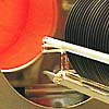
Our equipment at the EMRL in Aachen and Jülich comprises a broad spectrum of facilities for the fabrication and characterization of electronic materials and devices. The emphasis is placed upon oxide deposition technologies ranging from laser MBE, atomic layer deposition by MOCVD, high pressure sputtering to chemical solution deposition (CSD). These facilities are complemented by integration technologies such as optical and nanoimprint lithography, various metallization techniques, plasma based and ion beam based dry etching, as well as scanning probe based manipulation and self-assembly methods. In addition, we are equipped with a large variety of tools for the characterisation of processes, structures, and electronic properties. In particular, we provide a large range of dedicated scanning probe tools in order to analyze specific properties with atomic resolution. Circuit design is utilized for the development of hybrid and integrated circuits which comprise of new electronic functions as well as advanced measurement systems. Furthermore, our competences include numerical simulation and modelling methods which aim at the quantitative description of the electronic phenomena and materials under study as well as the corresponding devices.
The EMRL is a founding member of the section Fundamentals of Future Information Technologies of the Jülich-Aachen Research Alliance (JARA-FIT) and, as such, in addition to our own equipment, we have access through our partner institutes in the alliance to almost every conceivable nano-fabrication and nano-characterisation technique.
atomic scale deposition and self-assembly - electronic oxides and molecular systems

Our equipment at the EMRL in Aachen and Jülich comprises a broad spectrum of facilities for the fabrication and characterization of electronic materials and devices. The emphasis is placed upon oxide deposition technologies ranging from laser MBE, atomic layer deposition by MOCVD, high pressure sputtering to chemical solution deposition (CSD). These facilities are complemented by integration technologies such as optical and nanoimprint lithography, various metallization techniques, plasma based and ion beam based dry etching, as well as scanning probe based manipulation and self-assembly methods. In addition, we are equipped with a large variety of tools for the characterisation of processes, structures, and electronic properties. In particular, we provide a large range of dedicated scanning probe tools in order to analyze specific properties with atomic resolution. Circuit design is utilized for the development of hybrid and integrated circuits which comprise of new electronic functions as well as advanced measurement systems. Furthermore, our competences include numerical simulation and modelling methods which aim at the quantitative description of the electronic phenomena and materials under study as well as the corresponding devices.
The EMRL is a founding member of the section Fundamentals of Future Information Technologies of the Jülich-Aachen Research Alliance (JARA-FIT) and, as such, in addition to our own equipment, we have access through our partner institutes in the alliance to almost every conceivable nano-fabrication and nano-characterisation technique.
probing the nanoworld
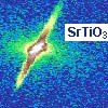
Progress in nanoscience and nanotechnology is closely related to the evolution of novel techniques in experimental analysis. Tip-based scanning probe systems represent the work horses of our equipment at the EMRL for probing nanoscale structures and objects with atomic resolution, comprising dedicated environments such as local conductivity microscopy (LC-AFM), tunneling microscopy (STM) and conductance spectroscopy (STS) of low-dimensional structure on oxide surfaces and of molecular systems, piezoresponse force microscopy (PFM) of polar oxide nanostructures and ferroelectric domain configurations, as well as nano-Raman and tip-enhanced Raman spectroscopy (TERS). This is complemented by looking into our electronic materials and fabricated nanostructures using our close ties with the Ernst Ruska-Centre for ultra-high resolution transmission electron microscopy and spectroscopy as well as with institutes of JARA-FIT which operate modern synchrotron beam lines for a multitude of analytical techniques for the investigation of structural and electronic properties of electronic materials.
measurement techniques
Our laboratories provide a wide variety of general and dedicated measuring systems for the electrical characterization of electronic thin film materials and demonstrator devices under controlled conditions (temperature, atmosphere, bias voltage, ageing history, etc.). Our equipment includes, for example, ultra-broad band impedance analyzers, ferroelectric and piezoelectric hysteresis set-ups, a double beam laser interferometer with a resolution down to 0.1 pm(!), ultra-fast transient analyzers for a temperature range between 4 K and 1500 K, microwave network analyzers, semiconductor parameter analyzers, electrochemical potentiostats, etc. A range of dedicated measuring systems has been developed in our labs and led to the foundation of the company aixACCT Systems GmbH in the year 2000, which successfully develops, produces, and sells customer-specific advanced measurement equipment. Today, the emphasis of our own development activities at the EMRL lies on the design and realization of complex ultra-high resolution scanning probe systems for dedicated applications.
circuit and system design

Analysis and design of circuits depends crucially on the utilisation of suitable tools for simulation and synthesis. The EMRL provides a professional infrastructure for the design and prototyping of measurement equipment at its disposal. This comprises design tools for ASIC design, FGPA design, and PCB design, a complete PCB prototyping facility, and test equipment for digital and analog circuit evaluation.
simulation and Modelling
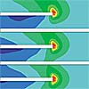
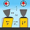
Modelling on different scales and with a variety of approaches are performed for phenomena, materials, and devices. Model-based numerical simulations are employed using both, self-developed program modules and commercial standard tools. The approaches comprise Finite Element/Difference Methods (FEM / FDM), Monte Carlo (MC) and Molecular Dynamics (MD) methods, as well as analytical calculations based on the band theory, the thermodynamics, and drift-diffusion transport theory. For example, we model the point defect disorder in oxides, electrostatic and electromagnetic fields by FEM/FDM, electron injection and transport on the microscopic scale of single molecules and on the macroscopic scale for metal-insulator-metal systems, redox processes and electrochemical metallization by MD methods. We cooperate closely with theory institutes in order to link our micro- and nanoscale simulation to ab-initio quantum mechanical models in which, e. g. local electron densities in crystal dislocation can be calculated on the atomic scale.
technological and analytical infrastructure